|
Simple DIY MIDI-to-CV Translator Box Another DIY project by M.J. Bauer |
|||||||||||||||||||||||||||||
___
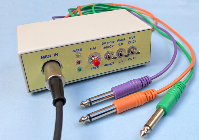 Front view of completed device. The paper decal was designed using Windows Paint. |
|||||||||||||||||||||||||||||
Index Disclaimer: The 'MIDI-to-CV Translator' is not a commercial product. The hardware design and software source code are in the public domain. The design may be replicated by suitably skilled electronics hobbyists. Detailed step-by-step instructions are not provided. The information published here may be used as a basis on which to design your own customized device. The author accepts no responsibility for any adverse consequences to makers attempting to replicate projects published on this website. There is no plan to sell fully-assembled modules, or a complete kit of parts. However, Gerber files for PCB fabrication are available to download. Also, bare (unpopulated) circuit boards may be offered for sale at cost price. Instalment 1 -- Overview There are other DIY MIDI-CV designs to be found and commercial products available at reasonable prices, so why would I design and build my own? The primary reason is that I want a device which is compatible with my EWI MIDI controller (REMI 2) which plugs into a MIDI IN socket (DIN-5) modified to supply 5V DC power to the EWI controller. This arrangement is called "Power-over-MIDI". There are other features I want in the device as well, not all of which are provided in other designs. But most of all, I like tinkering and making things. I don't care if I'm "reinventing the wheel". Here is my list of requirements (preliminary specification) for the device:
Provision of USB-MIDI comm's capability will allow the device to connect directly to a computer, enabling software app's (e.g. DAW or MIDI sequencer) to control analog synth's. Provision of a classic MIDI IN (DIN-5) connector allows any old MIDI keyboard or EWI MIDI controller to be plugged in.
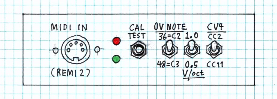
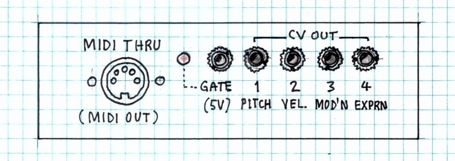
These sketches show what I have in mind for the front and rear panels...
The front panel (above) has 3 mini toggle switches to select modes of operation. The firmware can be customized to suit any particular requirements, of course, but this arrangement functions as follows: Switch #3 selects the "base note", i.e. the MIDI note number corresponding to 0.0V on the Pitch CV output. The 2 options are note 36 (C2) or note 48 (C3) to suit instruments covering the Tenor, Alto (Treble) and Soprano ranges. Switch #2 selects either 1 volt/octave or 0.5 volt/octave for the Pitch CV output. When 0.5 V/octave is selected, switch #1 setting is ignored and the "base note" is set to 12 (C0) or whatever else may be hard-coded in the firmware. The maximum CV output level is 5 volts, so the range is limited to 5 octaves when 1V/oct is selected. Switch #1 selects the MIDI message type associated with CV output #4 to suit the type of MIDI controller plugged in. An EWI controller (e.g. Akai 4000s, REMI 2, etc) sends Breath Pressure messages (CC2), whereas a MIDI keyboard may send Expression (CC11) or Channel Volume (CC07) messages. In any case, output CV4 would most likely be patched to a VCA control input on the synth to control the audio amplitude. Also on the front panel is a push-button switch. Its main function is to initiate a self-test/calibrate routine to check and adjust the CV outputs' volts-per-octave transfer characteristic. Another button function sets the MIDI channel number and Omni On/Off mode. If the button is pressed within 3 seconds following power-on, the toggle switches select 1 of 8 options encoded as a 3-bit binary number; i.e. 000 = Omni On, 001 = channel 1 (Omni Off), 010 = channel 2 (Omni Off), 011 = channel 3, etc. The 2 LEDs indicate the device status in the current mode of operation. (Details TBA.)
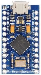
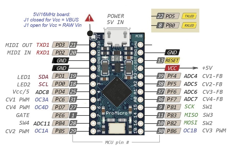
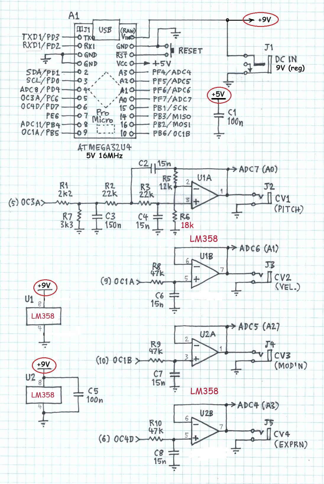
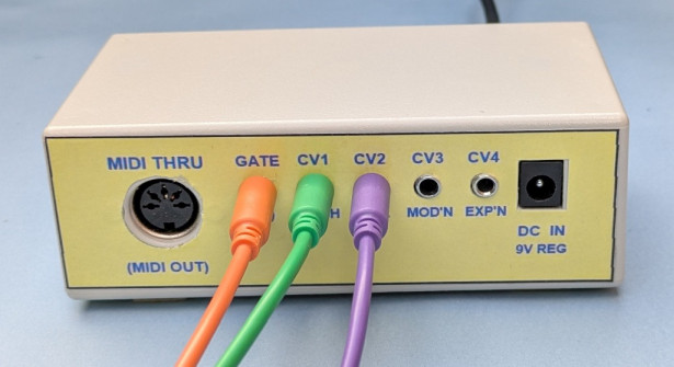
The rear panel has a 5-pin DIN socket which can function either as 'MIDI THRU' or 'MIDI OUT', selected by a hardware jumper. In 'MIDI OUT' mode, the transmitter is driven from the MCU (UART TX pin), so the firmware gets to decide what messages are sent, on what channel and when. (Details TBA.) A 'Gate' output (5V logic) and four CV outputs are provided on the rear panel using 3.5mm TS (mono) phone sockets. If you're patching into a Moog 'System 55' modular synth (for example), you'll need adapter cables with a 3.5mm plug at one end and a 1/4 inch phone plug at the other end. The four CV outputs are nominally 'Pitch', 'Velocity', 'Modulation' and 'Expression' to suit MIDI messages commonly implemented by MIDI controllers, including EWI's of course. You might want to substitute After-Touch for Expression on CV4, if you are using a keyboard which supports After-Touch. The yellow 'GATE' LED illuminates while the Gate output is asserted (High). I'm not sure yet how to handle Pitch Bend messages. What do commercial MIDI-to-CV devices do with Pitch Bend data? Do they provide a separate CV output, or is the Pitch CV output level adjusted according to the amount of bend (data in the Pitch Bend message)? For my purposes, I would choose the latter. Instalment 2 -- PWM 'DAC' Filter Design In this instalment I begin with a look at MCU I/O pin allocation. Does the Pro Micro have enough I/O for the application? Next I explain the trade-offs between PWM resolution, carrier frequency and filter response time. We'll see if the ATmega32U4 can meet the specified performance requirements. This image shows the MCU pin allocation. All required signals are catered for, without a single spare I/O pin!
What if there were not enough I/O pins? An easy solution would be to use an I2C I/O port expander, assuming only digital I/O's were needed. Adding analog inputs gets messy... that would involve a multiplexer. When a design crosses that line, it's often better to choose an MCU module with more I/O. Four analog inputs (A0..A3) will be used to measure the voltages on the CV outputs, in the self-test and calibration routines. The ADC can be configured to use the MCU's internal precision reference (2.56V) to measure the supply voltage (Vcc) on ADC8 (pin 4) via a 5:2 divider. PWM Resolution and Filter Response The CV output used to control synth oscillator frequency (pitch) needs to have high resolution. 16 bits would be ideal, but using a modest 8-bit MCU with a CPU clock frequency of 16MHz, a PWM resolution of 16 bits (1/64K) would allow a maximum PWM frequency of (16MHz / 64K) = 250Hz. This is way too low because the response time would be too long. Using PWM to make a D/A converter (DAC) requires the PWM "carrier" frequency to be eliminated. Practical (i.e. simple) low-pass filter circuits using a single op-amp are limited to 3rd-order designs, giving a roll-off slope of -60 decibels per decade. The attenuated PWM signal amplitude should be no greater than 1 LSb (least significant bit) of the DAC output at full scale. The PWM filter time-constant, i.e. reciprocal of the cut-off frequency,
is a fair measure of the response time, i.e. the time it takes for the
CV output voltage to respond to changes in the DAC digital value (PWM
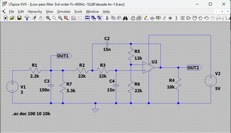
duty). So let's try for 12-bit resolution, which would be quite acceptable for the intended end-user application. The DAC LSb is about 1/4000th of full-scale, corresponding to a filter attenuation of 52dB. This is achievable with a 3rd-order filter, but what about the response time? With MCU timer clock freq = 16MHz, the PWM frequency is (16MHz / 4000) = 4kHz. For a third-order low-pass filter, 60dB attenuation occurs about one decade higher than the cut-off frequency, so Fc = (4kHz / 10) = 400Hz. This corresponds to a time-constant of 2.5ms which is in the right ball park. It's time to design a filter. From the foregoing theory, we know that the filter should have a cut-off frequency of 400Hz or higher and an attenuation of at least 52 decibels at the PWM frequency, 4kHz. I chose a 3rd-order filter comprising a 1st-order stage cascaded with a 2nd-order Sallen-Key configuration. You can find more theory here: To verify the filter design, I ran a simulation in LT-spice. The circuit is shown below. Normally the first stage would consist of only a resistor (R1) and capacitor (C3). However, to obtain the desired Butterworth filter characteristic, the pass-band gain, Av = 1.6. At high values of PWM duty, the op-amp output would clip at the +5V supply. To allow the full 5V output range, the PWM signal input to the filter must be scaled by a factor of 1/1.6. This is achieved by adding a resistor (R7) to form a voltage divider. But placing a resistor in parallel with capacitor C3 alters the filter frequency response, reducing the roll-off slope from -60dB per decade to -52dB/decade. Fortunately, this still meets the design criteria, as can be seen from the Bode plot.
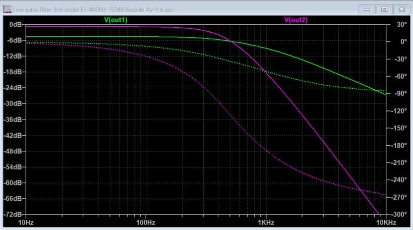
The composite 3rd-order filter frequency response is the solid magenta (pink) trace. The output amplitude at 4kHz is almost exactly -52dB, as required. The dotted trace is the phase shift curve which is of no great significance in this application. The green traces are for the first stage of the filter, taken from the high side of capacitor C3. Note that the pass-band amplitude is lower than that of the composite output due to the action of the voltage divider, R1 & R7 at the input.
Apart from verifying that it works as expected, another benefit of simulating a circuit before you build it is you can fiddle with component values to see how critical they are to the circuit's operation. For example, the filter pass-band gain is set by resistors R5 and R6. To obtain the optimal (flat) response, the gain (Av) should be 1.6 which means R6 should be 20k. I found that using the more common value of 22k made negligible difference to the filter response. Likewise, using 100nF for C3 made only a small change to the attenuation at 4kHz, i.e. 49dB instead of 52dB. The Pro Micro module provides 3 PWM pins capable of 12-bit resolution at 4kHz and another PWM pin giving 10-bit resolution at 16kHz. It would be possible to implement two more CV outputs with 12-bit resolution, but the other 3 CV outputs are not as critical as the Pitch output, CV1. Hence, in the interests of simplicity, I decided to make CV2, CV3 and CV4 all 10-bit resolution at 16kHz. Also, the response time of these 3 CV outputs is not as critical as CV1, so their filters can be a simple 1st-order RC circuit. Let's do the math again. A 10-bit DAC has LS bit = 1/1000th of full-scale. As noted earlier, the PWM filter attenuation should be a similar value. If we choose a CV response time of 5ms, the filter cut-off frequency is 200Hz. A 1st-order filter has a roll-off slope of -20dB per decade. Between 200Hz and 16kHz is roughly 2 decades, so we can expect an attenuation of about 40dB at 16kHz. 40dB represents 1/1000th of the pass-band output amplitude, so once again, conveniently, the design criteria have been met. Instalment 3 -- Circuit Design Contrary to an earlier decision to power the device from 5V via the USB port only, I have added an option to power it from an external DC supply with 9 volts regulated output. Using a supply voltage of at least 6V allows the Pro-Micro's on-board 5V LDO regulator IC to function, thereby providing a cleaner and more precise +5V line. For convenience to perform a firmware update, the device can still be powered from the USB port alone, but the CV outputs will not work. Part 1 of the schematic below comprises the Pro-Micro MCU module (A1), the 9V DC supply jack (J1), and the PWM filters for the CV outputs (explained in the previous instalment). Note that the circuit has been revised since the original blog post.
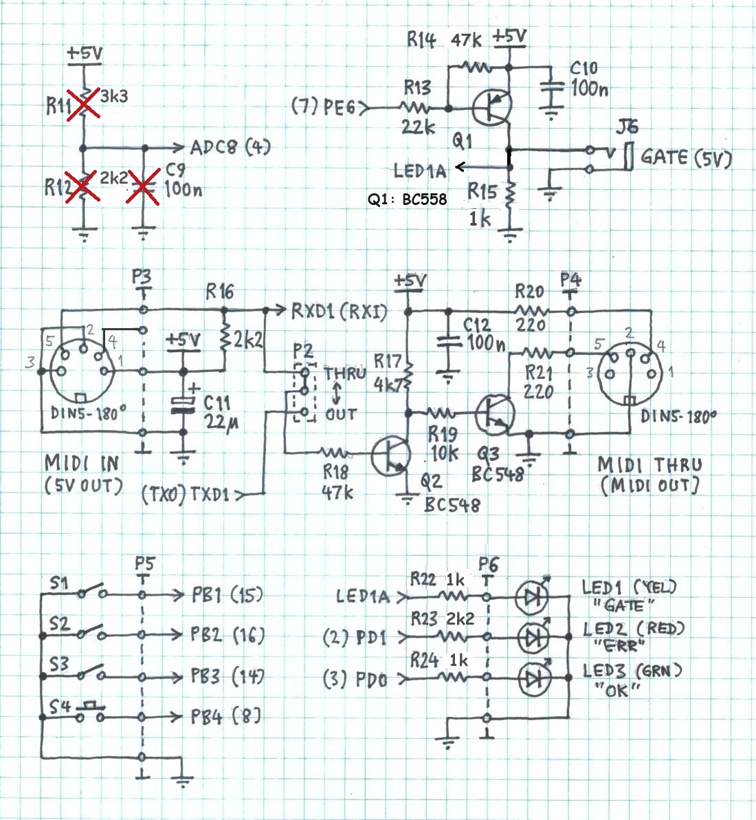
Provision of a reset button is highly recommended because the MCU bootloader firmware can execute differently depending on whether a power-on reset occurs or the reset button is pressed. The numbers in brackets beside MCU signal names are pin designators printed on the Pro-Micro module. These designators are a legacy from the Arduino pin labeling scheme which makes little sense in any other context. Part 2 of the schematic follows...
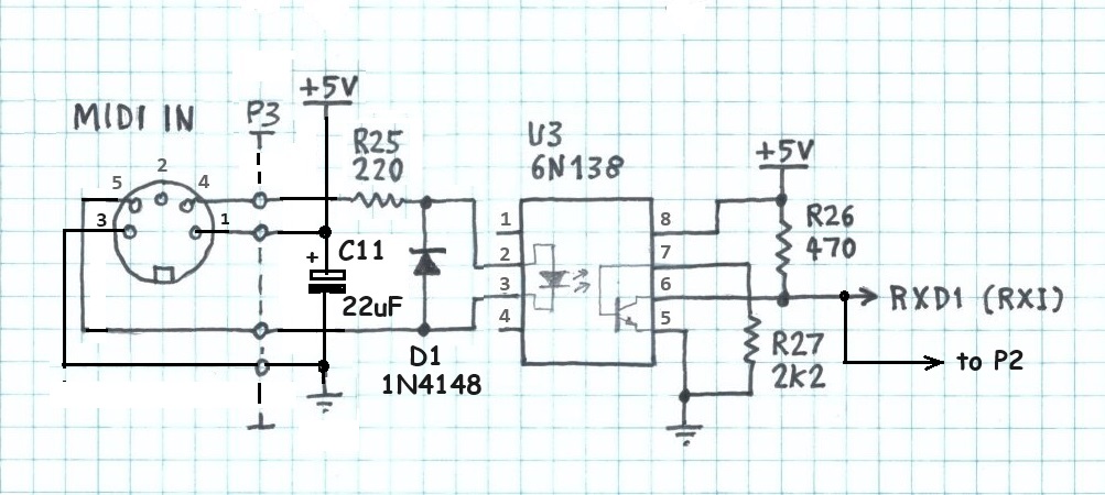
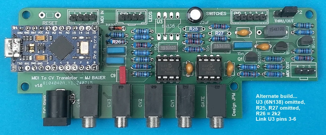
Pin PE6 of the MCU drives the GATE logic output. The pin is set Low to turn on transistor Q1 which asserts the GATE signal (High = +5V). R14 ensures Q1 is off when pin PE6 is high-Z, i.e. when the MCU is reset. The MIDI IN (receiver) circuit shown above is unusual. It was designed primarily to accept a REMI 2 EWI (MIDI wind controller). Thus, the circuit differs from a normal MIDI IN receiver in a couple of ways... 1. There is no opto-isolator! This means that a common (GND) connection is required between the attached MIDI controller and the MIDI-CV box. Pin 2 of the DIN5 socket is wired to GND for this purpose. (Pin 2 of a MIDI IN socket is normally not connected.) 2. The MIDI IN socket provides 5V power to the attached MIDI controller. This was implemented to power a REMI 2, but may also be used to power any MIDI device compatible with the Arduino "Power-over-MIDI" scheme (where DIN-5 socket pin1 = +5V, pin3 = GND). If you prefer to have a standard MIDI IN connection, use the circuit shown below, without +5V and GND wired to the DIN socket (pins 1 & 3). Alternatively, the 6N138 opto (U3) may be omitted, in which case bridge U3 pads 3 & 6, use 2k2 for R26 and wire DIN socket pin 2 to GND. R25, D1 and R27 can be omitted also. If a PCB design is produced, it will accommodate the "preferred" MIDI IN circuit shown here.
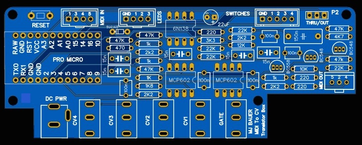
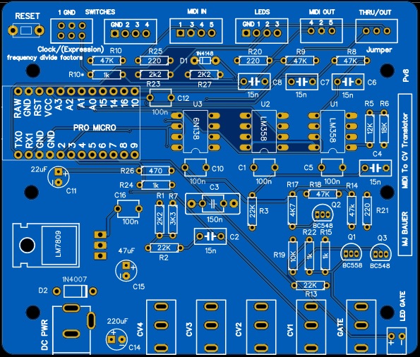
Preferred MIDI IN receiver circuit using opto-coupler The MIDI THRU/OUT transmitter circuit is unremarkable. Jumper P2 selects between MIDI THRU and MIDI OUT operation. I have not yet contemplated any specific function for the firmware-driven MIDI OUT option. Instalment 4 I am excited to announce that a Synth-DIY fan and regular correspondent, Jean-Pierre (in France), has designed a PCB for the MIDI-CV project. The board has all thru-hole components to make it easier for those not skilled in SMT assembly. Here is a picture of the final layout...
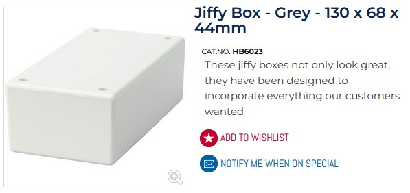
The PCB is designed to suit either a stand-alone box or Euro-rack module. Be sure to notify me if you are interested in obtaining a board... Ordering details here For a stand-alone module, the PCB fits nicely into a plastic "Jiffy Box", size 130 x 68 x 44 mm, sold by Jaycar (in Australia) in light-grey or black, priced at AU$4.50 last time I checked.
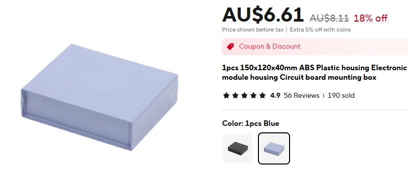
I found another suitable box on AliExpress. This type is available in black, grey or (cool) blue.
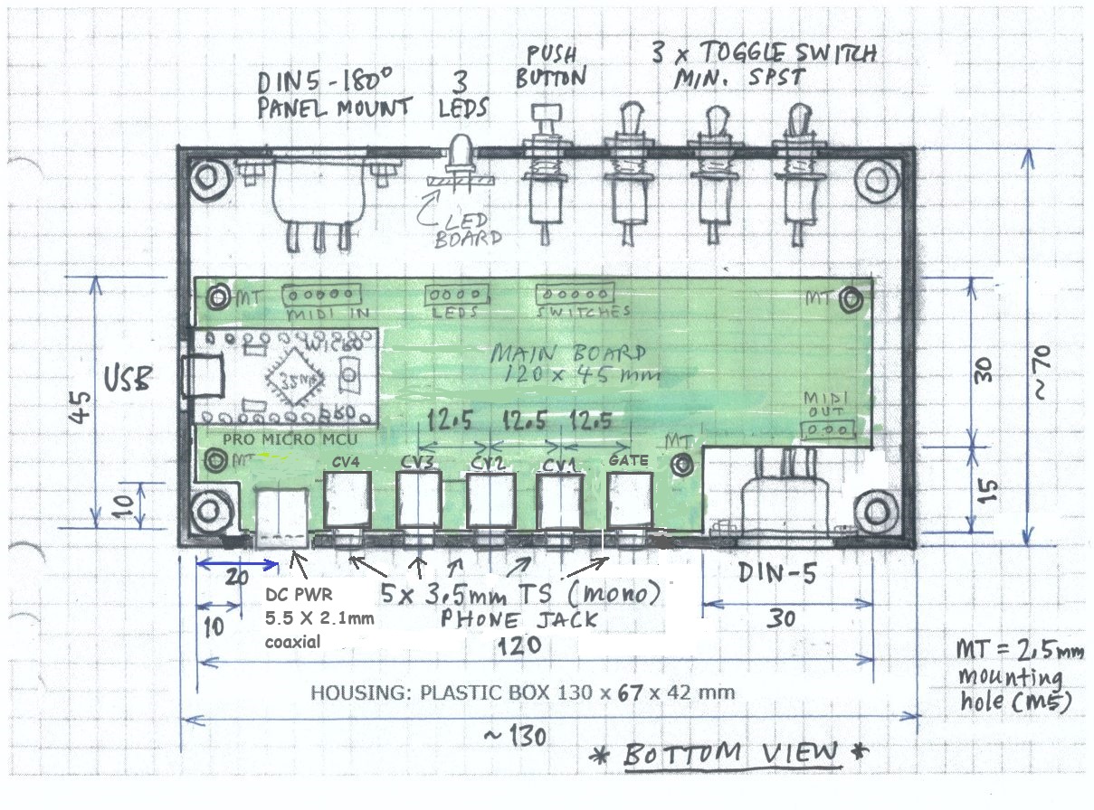
Below is a rough sketch of the proposed internal layout of the box, viewed from the under-side. The lid attaches to the bottom. The PCB is mounted on the top panel of the box on 6mm long spacers, held in place with machine screws. The board can be easily removed and replaced for rework, if required. The DIN connectors, toggle switches, LEDs and push-button are mounted on the box panels, wired to the board via SIL headers. This arrangement, contrary to using PCB-mounted parts, allows various alternative enclosures. It also allows more flexiblity for makers to rearrange the front panel layout as desired. A Euro-rack module can be contructed by mounting the switches, LEDs and MIDI IN socket on the front panel vertically, alongside the row of 3.5mm TS jack/sockets fitted on the PCB. Don't fit the DC power inlet socket. Wire a 2-pin polarized in-line connector (e.g. Molex) to supply 9V DC from inside the rack.
Instalment 5 -- Assembly Download the Parts List and start to source parts while waiting for your PCB to be delivered. An assembled circuit board is shown here. Apart from the Pro Micro MCU, a couple of dual op-amps and a few connectors, there's not much in it... except quite a lot of resistors (but they're cheap). You can use smaller resistors (1/4W or 1/8W) if you prefer. The board was not really designed for 1/2W resistors, but they fit OK. Take care not to stress the resistors when bending their leads. As noted before, there is an option to omit the opto-coupler (U3) from the MIDI IN circuit. If you choose this option, be sure to wire pin 2 of the MIDI IN socket to GND. Other modifications are noted in the picture. Pins 1 and 3 of the DIN5 socket should be left unconnected, except if your MIDI controller uses "Power-over-MIDI" (e.g. the "REMI 2" EWI controller).
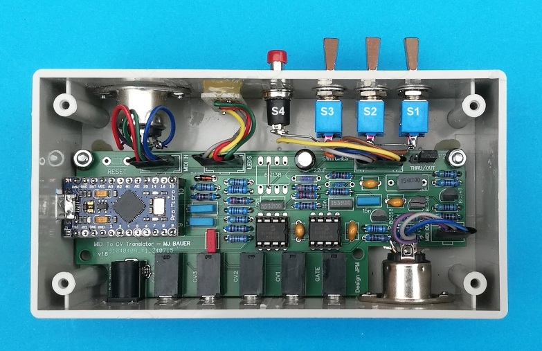
I used cheap pin-headers made by breaking up a 40-pin strip. Likewise, the matching "plugs" were made from a 40-way socket strip... the same as used for the MCU module "socket". You can use more elegant polarized SIL pin-headers and plugs if you prefer. There is no RESET button on the board shown above because I did not have one of the right type. However, I recommend to fit a RESET button. A few wire harnesses need to be made to connect the DIN5 sockets, LEDs and switches to the PCB. The LEDs were soldered onto a little piece of perf-board. Note that toggle switch S1 is in the rightmost position, S2 in the middle and S3 to the left. The push-button is designated 'S4' on the schematic. When the circuit board is complete, measure the positions of the jacks along the rear panel, and the USB socket on the LH side. Cut holes in the enclosure to fit all parts which poke through the panels. The circuit board is mounted in the enclosure (Jiffy Box) on 6mm stand-offs (spacers). Only 2 mounting points are needed, near the 2 rounded corners of the PCB, because the 3.5mm CV-out jacks will hold the board in place on the opposite side (against the rear panel). I recommend to fix the 6mm stand-offs in place using hot-melt glue. Otherwise, they are a pain to keep in place while inserting the mounting screws. The LED board also may be fixed in place with hot-melt glue. If you're using the "standard" enclosure (Jiffy Box), the assembled device should look something like this...
Jiffy Box with bottom cover removed Labeling of switches, connectors, etc, on the front and rear panels may be done with a label-maker of the type that works with self-adhesive transparent film tapes. Another method which I often use is to draw panel decals using Windows Paint (or Paint-Shop Pro), print actual size in colour on paper, cover with transparent adhesive film (e.g. bookbinding film), cut holes for switches, sockets, etc, then glue it onto the box.
Rear view of completed device <!> PCB and circuit mod's The PCB (v1.6) has signal RXD1 (U3 pin6) routed to pin2 (centre pin) of jumper header P2. However, U3 pin6 should be routed to pin1 of P2. Break the track which connects to R18 (47k) on the top side of the PCB. Solder a wire from U3 pin6 to P2 pin1 (under-side). Also, there is a "track link" bridging pins 1 & 2 of P2 (top-side) which must be cut if the MIDI OUT option is selected. The circuit was revised to overcome a limitation of the original op-amp chosen, MCP602. Although the MCP602 output voltage range is spec'd as "rail-to-rail", the common-mode input voltage range only goes as high as Vdd minus 1.2V, meaning the output voltage could not go higher than about 3.6V in this filter configuration. A higher Vdd would fix the problem, but the MCP602 maximum supply voltage is 5.5V, so this device is not suitable. The simplest work-around was to substitute a different op-amp, LM358, which is pin-compatible, dirt cheap, allows common-mode input voltage down to 0V, and will operate at a higher supply voltage. The schematic and parts list have been amended accordingly. The circuit revision requires a few minor hacks to the PCB v1.6, as shown in the pics below. Cut tracks where indicated by red ellipses and solder wire links on the under-side. Resistor
R6 should be 18k (marked 22k on PCB v1.6). The original value (22k) did
not provide enough gain to compensate for the filter input voltage
divider (R1, R7). See picture for location
of
R6. 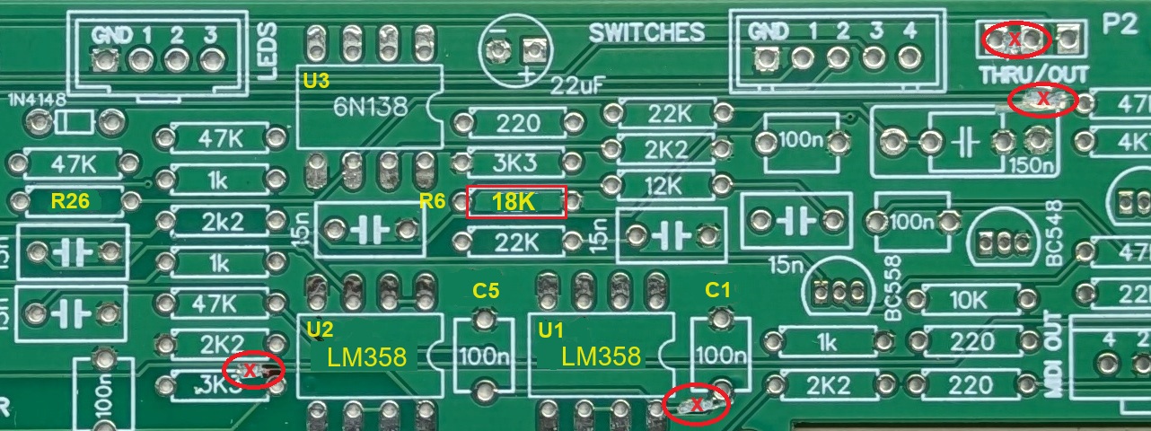 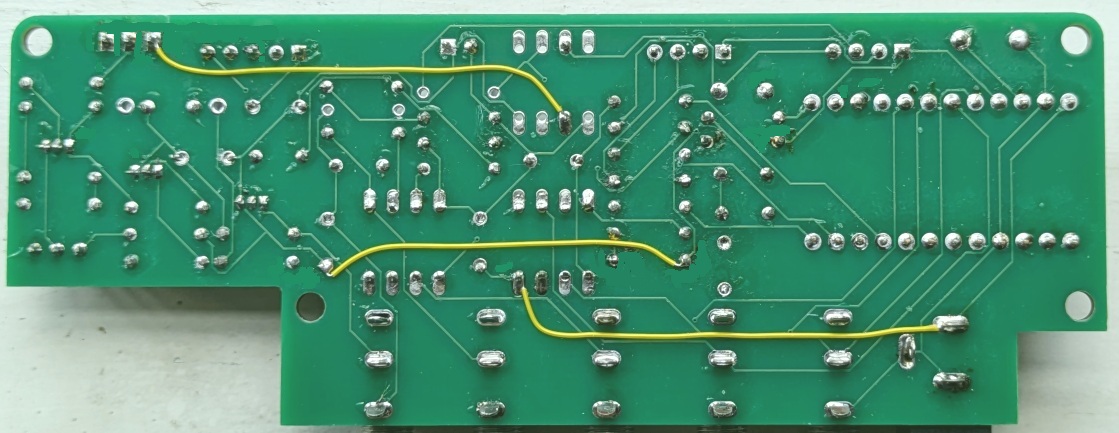 The circuit revision means that the MIDI-CV box needs to be powered from a PSU with a 9V regulated output, although it will function properly down to 7.5V. It's probably best not to go higher than 9V, because the Pro Micro on-board 5V linear LDO regulator IC could overheat and burn out. The device can still be powered via USB for firmware loading. Lastly, due to inadequate precision of the MCU ADC internal voltage reference, resistors R11, R12 and capacitor C9 are no longer required and may be omitted. (See "Performance and Design Improvements".) Firmware Download the Firmware pack here A hex object file is included so you can program the device without needing to re-build the firmware. The board can be programmed via the USB port without needing Microchip/Atmel Studio (IDE) and without a hardware programming tool. Proceed as follows... The Pro Micro board has a flash-resident AVR bootloader. A Windows application called “AVRdude” communicates with the bootloader via USB to program firmware into the MCU flash memory. Hence you need to download some files to run "avrdude" on Windows. The best place to download the files is GitHub, here: https://github.com/mariusgreuel/avrdude/releases. There should be 3 distribution files: “avrdude.exe”, “avrdude.conf” and “avrdude.pdb”. Copy these files to a new folder named “AVRdude” on your PC local drive, in the “root directory” (C:\). Connect your board to a USB port on your PC. Open Windows “Device Manager” utility and click on “Ports (COM & LPT)”. Immediately after you apply power or reset the MCU, you should see the board’s USB-serial device listed. Note the number of the associated “COM” port. Be aware that the COM port number may change from time to time. Always check the allocated COM port after re-connecting the board to your PC. Copy the hex file "MIDI-to-CV-translator-v1.0.hex" into the folder "C:\AVRdude". You can enter the command first and then reset the MCU, if you prefer, because avrdude will keep trying to establish comm's with the bootloader, indefinitely. If all goes well, avrdude will report success. Note: When
AVRdude finishes the firmware loading process, it may be necessary to
remove the USB cable, then re-apply power to the device to start the
user program. To modify or extend the program... The firmware download package includes source code, libraries and all project files needed to build the program using Microchip/Atmel Studio IDE for AVR and SAM Devices. Download and install the app. Create a
project folder on your Windows PC local drive named "MIDI-to-CV-translator".
The "solution" file expects this name exactly. Copy all the files from
the distribution pack, "MIDI-to-CV-firmware-pack.ZIP" to your
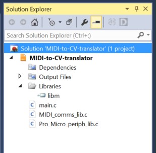
project folder. If Atmel Studio is already open, close it. Double-click the file "MIDI-to-CV-translator.atsln" in the project folder. Atmel Studio will open the "solution" (project). Check that all required "components" (files) are present and in the correct place, as can be verified in the "Solution Explorer" pane (see screen-shot below)...
To view/edit a source file, click the file-name in the Solution Explorer pane. When you're done editing the source code, assuming everything is correct, click 'Build Solution'. If the build was successful, a hex object file "MIDI-to-CV-translator.hex" will be placed in the project sub-folder "..\Debug". To program the board, you have a choice between two options. Probably the easiest method is to proceed as above using AVRdude stand-alone from Windows Command Prompt. Another option is to create a "software programming tool" in Atmel Studio. This method allows you to program the board directly from within Atmel Studio. Proceed as instructed in the linked document, here... How to program the Pro-Micro board via USB using Atmel Studio IDE Additonal notes on Pro Micro USB bootloader variants Some Pro Micro boards have the Sparkfun (modified) bootloader installed. This behaves a little differently compared with the "normal" Arduino Micro/Leonardo bootloader. To enter bootloader mode (and remain in the bootloader for 10 seconds) press RESET twice in quick succession. Otherwise, a reset should start the user application program. In case of the Arduino Micro/Leonardo bootloader (installed in most Pro
Micro clones), the MCU enters bootloader mode immediately on
power-up (and/or reset) and remains in bootloader mode for 10
seconds. After 10 seconds, the bootloader tries to start the user
application program, if any is loaded. User Guide Power Supply Requirements The
MIDI-CV box should be powered from a PSU with 9V regulated DC
output, although it will function properly down to 7.5V. Do not exceed
9V, because the Pro Micro on-board 5V linear LDO regulator IC
could overheat and burn out. The risk is higher where the MIDI-CV box
supplies 5V power to external devices via the "power-over-MIDI"
connection. The default MIDI IN configuration is Omni-ON, meaning that the device will respond to incoming messages addressed to any MIDI channel. To change the configuration, power down the device and set the 3 toggle switches to select the required MIDI IN mode and channel (1..7) as in the table below. (Switch position 0 = down/closed, 1 = up/open.) Press and hold the CAL/TEST button, power up the device, then release the button. The configuration is preserved in non-volatile memory (EEPROM), but it may be defaulted when the firmware is updated, depending on the Pro Micro bootloader operation.
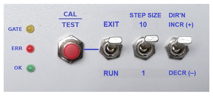
Self-test / Auto-calibration Every time the device is powered up, if a manual calibration has not been performed, it will perform a self-test and CV1 auto-calibration routine. This takes less than a second. If a fault is detected, the red "error" LED will remain lit. Otherwise, the green LED will illuminate indicating that the unit was calibrated successfully. Calibration accuracy can be checked by measuring the voltage on CV1 after a normal power-up, without any MIDI input being received. The CV1 output should read 2.50 volts. Factors affecting CV1 accuracy are primarily the error in AVCC (+5V from Pro Micro LDO regulator) and the PWM filter DC gain error (determined by R1, R7, R5 & R6). Manual calibration makes the accuracy of CV1 immune to these sources of error. Manual Calibration (requires firmware v1.2 or later) Precision of the self-test auto-calibration routine is limited by the accuracy of the ADC voltage reference, AVCC (= Vcc). The manual calibration method improves the accuracy of the CV1 output. All you need is a good quality digital voltmeter or DMM (preferably 5+ digits, but a 4-digit DMM is OK). The manual calibration routine is started by closing switch S3, then press the CAL/TEST button. Monitor CV1 output voltage with your voltmeter. It should be somewhere around 4V initially. The aim is to use the other 2 switches with the button to "jog" the reading on CV1 as close to 4.000V as you can get. This picture shows the switch functions in calibrate mode...
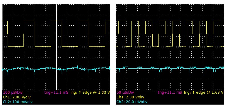
The green "OK" LED flashes at 1Hz while the cal routine is running. Each time the button is pressed, CV1 output voltage will increment or decrement, one "step" at a time. The step size (1 or 10 units) is selected by switch S2. The step direction (up or down) is selected by switch S1. When the output voltage reads 4.000V (as near as possible), open switch S3 and then press the button to exit the routine. That's it... the CV1 output is now calibrated! Once a manual calibration has been performed, the self-test auto-calibration function will not be performed at start-up. Calibration parameters determined by the manual procedure are preserved in EEPROM, so it should not be necessary to re-calibrate, except if a hardware change impacts CV1 accuracy, e.g. the MCU is replaced, or if an external load connected to CV1 has a very low input impedance (< 2k ohm). GATE output function in Legato mode The GATE signal (5V logic output) is intended to control one or more "ADSR" envelope generators in the attached synthesizer. The leading edge of the GATE signal triggers the "Attack" segment of the EG which progresses automatically through the Decay and Sustain segments. When the GATE signal is negated (Low) the Release segment of the EG should activate. This MIDI-CV Translator is designed for use with monophonic analog synth's. As such, it complies with the MIDI 1.0 Specification (v4.2 1995) with regard to "Legato" operation. If your MIDI keyboard, sequencer, or whatever, is polyphonic and the MIDI-CV module is set to Legato mode, it will emulate the behaviour of a MIDI-compliant monophonic keyboard/controller. This mode of operation is compatible with glissando or portamento functions which may be supported by your synth. Legato emulation mode works as follows: If a MIDI Note-On message is received while the GATE signal is negated (Low), i.e. while there is no note keyed, then the GATE output will be asserted (set High) and the Pitch CV output will be set according to the MIDI note number received. The Velocity CV output will also be set according to the MIDI data value. This should cause any gate-activated EG(s) on the attached synth to enter the Attack phase. If a MIDI Note-On message is received while the GATE signal is asserted (High), i.e. while a prior note is already keyed, the GATE output will remain asserted (High). However, the Pitch CV and velocity CV outputs will be updated according to the new MIDI note data received. This is a Legato note change. If a MIDI Note-Off message is received and the MIDI note number is the same as the note keyed prior, i.e. the note that was first initiated, the GATE signal will be negated (set Low). The same response is executed if a MIDI Note-On message is received with Velocity value zero. (This is equivalent to Note-Off.) If a MIDI Note-Off message is received and the MIDI note number is different from the note keyed prior, the GATE output will remain asserted (High). The Pitch CV output will be updated according to the note keyed prior, i.e. before the note identified in the Note-Off message. This is also a Legato note change. GATE output function in "Multi-Trigger" mode (Legato Off) [Firmware v1.x only] -- Your MIDI controller may send a Control Change 68 ("Legato Foot-Switch") message to disable or enable legato. A data value of 64 or higher represents "Legato On"; a value 63 or lower represents "Legato Off". The Legato on/off setting is persistent across power-downs. Multi-trigger mode should be selected if your MIDI controller (keyboard, sequencer, etc) is polyphonic and you don't want to emulate monophonic keyboard operation. If a MIDI Note-On message is received while the GATE signal is already asserted (High), i.e. while a note is keyed, then the GATE output will be negated (set Low) momentarily. After a short delay (5 milliseconds), the GATE output will be re-asserted (set High) and the Pitch CV output will be updated according to the new MIDI note number received. Likewise, the Velocity CV output will be updated. In Multi-trigger mode, all notes keyed will result in a GATE pulse (leading edge transition), ensuring that the synth envelope generator(s) will start a fresh 'Attack' segment. --See also Instalment 8 below. Pitch CV Output The Pitch CV output signal is updated whenever a MIDI Note-On message is received. The range of notes corresponding to the full-scale output voltage (+5.0V) depends of a couple of front-panel switches. The range is obviously limited to 5 octaves when 1V/oct is selected. Switch S3 selects the "base note", i.e. the MIDI note number corresponding to 0.0V on the Pitch CV output. The 2 options are note 36 (C2) or note 48 (C3) to suit instruments covering the Tenor, Alto (Treble) and Soprano ranges. Switch S2 selects either 1 volt/octave or 0.5 volt/octave for the Pitch CV output. When 0.5 V/octave is selected, switch S3 is ignored and the "base note" is set to 12 (C0). Velocity CV Output The Velocity CV output signal is updated whenever a MIDI Note-On or Note-Off message is received. Full-scale output (+5.0V) corresponds to a velocity data value of 127. The MIDI-CV device does not perform any transfer function, e.g. exponential, on the data value. This should be a function of any synth module(s) using velocity as a control input. Modulation CV Output The Modulation output (CV3) responds to MIDI Control Change 01 and 33 ("Modulation wheel/lever") messages. The data value may be 7 bits (CC01) or 14 bits (CC01:CC33) where CC01 provides the high-order 7 bits (MSB) and CC33 provides the low-order 7 bits (LSB). In any case, a data value of 127 (MSB only) or 16,383 (14-bit data value) corresponds to full scale, i.e. +5.0V output on CV3. Note that Modulation data is unipolar, ranging from zero to full-scale. Expression CV Output The "Expression" output (CV4) responds to either MIDI Control Change 02 ("Breath Pressure") or Control Change 11 ("Expression Pedal") messages. The data value may be 7 bits (CC02 or CC11, high-order byte only), or 14 bits where CC34 or CC43 provides the low-order 7 bits (LSB). In any case, a data value of 127 (MSB only) or 16,383 (14-bit data value) corresponds to full scale, i.e. +5.0V output on CV4. Expression data is unipolar, ranging from zero to full-scale. The MIDI-CV device does not perform any transfer function, e.g. exponential, on the data value. This should be a function of any synth module(s) using CV4 as a control input. A firmware variant will include an option to utilise switch S1 to select between two functions for the output CV4, i.e. 'Expression' CV (as above), or a 'Clock' signal which responds to MIDI 'Timing Clock' messages. -- See also Instalment 8 below. Pitch Bend MIDI Pitch Bend messages, when received, adjust the Pitch CV output voltage according to the Pitch Bend message data value (14 bits) and a "Pitch Bend Sensitivity" parameter. Pitch Bend data is unipolar (unsigned) ranging from 0 to 16K (0x3FFF). Pitch-bend controls typically have a "centre zero" mechanical design, so that a bend value of 8K (0x2000) represents zero change in pitch. The full-scale data value (16K) corresponds to the extreme limit of movement of the control in the forward direction. The actual change in pitch corresponding to the full-scale data value in a Pitch Bend message is determined by a parameter called the "Pitch Bend Sensitivity" (aka "Pitch Bend Range"). This parameter may have units of cents (1/100 semitone) or semitones. A MIDI message exists to set the "Pitch Bend Sensitivity". Actually, two messages are required: Control Change 100 ("Registered Parameter") with data value of 0 (defined as "Pitch Bend Sensitivity"), followed by a Control Change 6 (Data Entry) with data value representing the required sensitivity in semitones. For example, to set the Pitch Bend Range (sensitivity) to one octave, the data value in the CC6 message would be 12 (semitones). The firmware "default" value for Pitch Bend Range is 2 (semitones). The Pitch Bend Range parameter value is "remembered", i.e. the setting is persistent across power-downs. Instalment 7 Performance and Design Improvements With regard to CV output voltage range, linearity and noise, the MIDI-CV box meets my expectations, although the amount of residual PWM carrier on the CV1 output is a little higher than ideal. However, most synth VCO's would be unaffected by this amount of noise, I guess. The PWM "noise" is most likely due to poor performance of the active low-pass filter, which could be improved by using a better op-amp than the crappy old LM358, for example LM2904. The 'scope shots below show the CV outputs' noise performance. The yellow traces are the PWM signals at MCU pins OC3A and OC1A. The blue traces are the CV outputs, AC-coupled to the 'scope. On the left is CV1 which has a noise amplitude of about 20mVp-p (~7mV RMS). The vertical scale is 100mV per division. On the right is CV2 with a noise amplitude less than 6mVp-p (~2mV RMS). The vertical scale is 20mV per division.
Manual calibration of the Pitch control output, CV1, is now implemented in the firmware (v1.2+). Finally,
rest assured that this MIDI-CV Translator performs quite well without
compensation for error in the ADC reference. The Pro Micro on-board 5V
LDO regulator is reasonably accurate... in fact much more accurate than
the ATmega32u4 internal reference! Most synth VCO's
have a "fine tune" control, so any error in the CV1 output voltage
can be compensated by tuning the VCO frequency.
Vintage synth VCO's required frequent calibration and tuning
to obtain anything near "concert pitch" from their analog keyboards. Instalment 8 (Addendum - November 2025) Adding a CLOCK (SYNC) Pulse Output Analog sequencers, sample-and-hold modules, etc, may need to be synchronized to a MIDI "master" controller. Some commercial MIDI-CV modules provide a clock/sync output jack. The clock signal is a digital pulse which is generated whenever a MIDI "Timing Clock" message (F8 hex) is received. The MIDI "Timing Clock" message frequency is typically 24 times the "beats per minute" (BPM) rate, assuming the beat interval is one "quarter note" (aka crotchet). Example: At 120 BPM (allegro!) the MIDI clock rate is 24 x 120 pulses per minute = 48 Hz. The MIDI clock rate may be too high for the analog sequencer or whatever is be synchronized, so some MIDI-CV converters have an option to divide the clock frequency by a factor, e.g. 2, 3, 4, 6, 8, 12, 24. A clock output can be easily added to my DIY MIDI-CV translator device. If it is inconvenient to add an extra TS jack/socket for a clock output, you can repurpose the CV4 output for the clock. With a simple hardware mod, the CV4 jack can be made switchable between 'Expression' and 'CLOCK' outputs. For use as a clock output, the PWM filter time-constant (T = 5ms) applied to CV4 is too high. The clock pulse (typically 1 or 2 milliseconds) would be snubbed out. If you don't an 'Expression' output, the simplest option is to replace resistor R10 (47k) with 1k, or just solder a 1k in parallel with the 47k. If you want to be able to switch the function of CV4 between 'Expression' and 'CLOCK' output, switch S1 can perform this function, but you'll have to replace it with a double-pole switch. One pole switches R10 between 1k and 47k. The other pole retains the original connection to the MCU (I/O pin PB1) to signal to the firmware which position the switch is in. Firmware version 2.0 supports this function, i.e. CV4 output is switchable between 'Expression' or 'Clock' using switch S1. The original usage of S1 is no longer supported. If CV4 is set to 'Expression', the output signal will respond to either or both MIDI CC02 and CC11 messages. Alternatively, if you have no need for an 'Expression' CV output, it can be replaced permanently with the clock function. Resistor R10 is replaced with 1k. Switch S1 could be used to choose between two clock frequency divide factors, for example 6 or 12. Selection of "Keying Mode" -- Multi-trigger or Legato This DIY MIDI-to-CV translator was designed for use with a monophonic analog synthesizer. The MIDI Specification v1.0 explains how a monophonic synth should respond to Note-On and Note-Off messages received from a compliant monophonic MIDI keyboard or controller. There is no specified behaviour for a monophonic synth controlled by a polyphonic keyboard or sequencer. Consequently, the synth behaviour may not be what's expected or required. There are two ways around this anomaly. The first is to use a compliant monophonic keyboard or sequencer, but many MIDI keyboard controllers and sequencers are polyphonic, without an option to select monophonic operation. The second (preferred) work-around is use a MIDI-CV translator module which can operate in either "Legato" mode or "Multi-trigger" mode for use with polyphonic controllers. Switching between Legato or Multi-trigger modes was always possible in firmware version 1.x, but the switch was made by a MIDI CC68 message. Not all MIDI controllers support this message type, or perhaps not conveniently. Hence, firmware version 2.0 is changed so that switch S2 selects between Legato or Multi-trigger mode. Close S2 to select Legato mode; open S2 to select Multi-trigger mode. The MIDI CC68 message type is no longer recognised. See the User Guide for details of Legato and Multi-trigger operation. If you want a custom firmware variant, but your C coding skills are not up to par, send me an email request and I'll be happy to provide assitance or do the programming for you. ___ 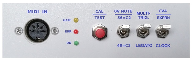 Front panel markup to suit firmware version 2.x ___ How to obtain a circuit board Bare (unpopulated) PCB's may be available for purchase from the author. Cost price is only about $3, but postage outside Australia is not cheap. For example, to send a parcel (up to 250g) to the USA costs US$15. However, to send an ordinary letter (same size and weight) costs only US$3. Go figure! Anyhow, I have posted PCB's overseas successfully as an "ordinary letter" in a plain envelope. If you are willing to accept the risk that delivery could go astray, send me an email to request PCB availability, price and postage fee to your country. It may be more cost-effective to get your own boards fabricated in China. Download Gerber files for PCB fab here ________ Update (2025-11): Jean-Pierre has designed an alternative PCB which is suitable for larger boxes and for mounting in a Euro-rack module. This PCB has an on-board 9V regulator IC, so the module can be powered from 12V DC. Latest revision of Gerber files to fabricate the PCB are available on request. ___ Thanks for taking
an interest in this project. I hope the design suits your requirements.
Otherwise, perhaps you will get some ideas for your own design. Feel
free to send comments and queries. |
|||||||||||||||||||||||||||||
|
Send email enquiries, comments, suggestions, PCB orders, etc, to...
Last update: 16-NOV-2025 ___ |